Quantcast
Channel: Cadence PCB Design Blogs
Viewing all 663 articles
Browse latest View live

What's Good About Allegro PCB Editor Find Filter Support of Hierarchical Constraint Objects? 16.6 Has It!

$
0
0

The 16.6 Allegro PCB Editor release ‘Find by Name’ list now supports hierarchical database objects - Diff Pair, Match Group, Region, for example:

16.5 Find by Name:

16.6 Find by Name:

Read on for more details …

Invoke the ‘Assign Color’ command.

Select ‘Diff Pair’ from the ‘Find by Name’ list.

Click the ‘More’ button.

Select a few Diff Pairs from the left-side pane; once selected, they appear in the right pane.

Click OK:


Another selection method you may want to consider is to enter any Application Mode and RMB – Selection Set - Object Browser:


I look forward to your comments.

Jerry “GenPart” Grzenia


What's Good About Allegro PCB Editor Highlight Nets Associated with Component? It’s in the 16.6 Release!

$
0
0

With the 16.6 Allegro PCB Editor release, a simplified method to highlight or de-highlight all nets associated with a component is offered in all applications modes. Hover over a symbol(s), then use the RMB to access the ‘Highlight Associated Nets’ command. Nets assigned the DC Voltage property are ignored.

Here are the steps to accomplish highlighting nets:

  1. Using any one of the application modes, hover over a symbol.
  2. Use the RMB to access the Highlight associated nets command.
  3. Select a highlight pattern from the popup dialog.
  4. De-highlight all associated nets by hovering over the symbol, then RMB - Dehighlight associated nets.

If the nets are not highlighting, check to see if the ‘display_nohilitefont’ variable is set.

Please share your experiences with this new capability.

Jerry “GenPart” Grzenia

Customer Support Recommended—Design and Simulation of Full Bridge DC-DC SMPS Using AMS Simulator

$
0
0

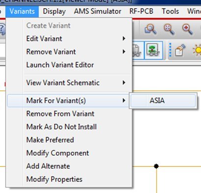
Switched Mode Power Supplies (SMPS) are used extensively in most of the power conversion processes due to their efficiency and compactness. The analysis, design, and the modeling processes have all grown in the past four decades. Most of these developments were centered on hard-switching converters where the switching frequency was limited to a few KHz. The present direction of evolution in SMPS is towards high efficiency and higher power conversion density. These twin objectives demand high switching frequency and low overall losses. The designing and testing of SMPS is cumbersome work and require lots of trial and error methods to get the right output.

Allegro AMS Simulator (PSpice) gives you an option to reduce your effort by simulating your design before going for the real hardware design. The following is an excerpt from an app note* that provides details on designing and simulating SMPS using AMS Simulator with a real-time test circuit.

Introduction

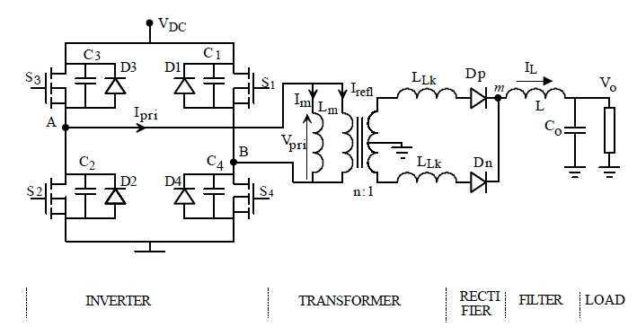
The full-bridge topology of the DC-to-DC power transformer is an electrical bridge between the junctions of four MOSFETs, M8, M9, M10, and M11, as shown in Figure 1.

Figure 1: Full-Bridge DC-to-DC Converter 

MOSFETs M8 and M11 are switched on simultaneously for an adjustable time during one half period. MOSFETs M9 and M10 are switched on simultaneously for an equal time during the alternate half period. The transformer primary voltage is a square wave DC voltage supply.

Topologies vary as per the desired output voltages, for various power ranges. Multiple switch topologies are generally used for high-output power applications. These switched-mode power supplies operate in the frequency of a few KHz to MHz range. There is a growing trend of increasing the switching frequency.

Circuit Analysis

Figure 2 shows a schematic diagram of a full-bridge DC-to-DC converter used for analysis and simulation. Capacitors C1 to C4 represent the output capacitances of the MOSFET including any external snubber capacitors that are added. Lm and LLk represent the magnetizing and leakage inductances, respectively, of the transformer.

Figure 2: Schematic Diagram of Full-Bridge DC-to-DC Converter 

For the purpose of analysis, a complete cycle of operation is divided into eight distinct intervals for the inverter. These cycles are covered in detail in the app note*.

Sample Circuit and Simulation Results 

Specification:

  • Input voltage: 27V
  • Output voltage: 270V
  • Output power: 400W
  • Output load: 1.5Amp
  • Switching frequency (fs): 50KHz 

Design Process

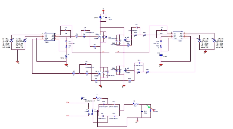
A schematic diagram of the power converter is shown in Figure 3.

An input of 27V DC is given to the full-bridge converter. Switching the action of the inverter will apply voltages of +/-27V to the primary of the high-frequency transformer during each half cycle. The transformer operates at a frequency of 50KHz. IR2011, used as gate driver, is a high-power, high-speed MOSFET driver that has a floating channel up to 200V and a gate driver supply voltage range of 10V to 20V. It has a matched propagation delay for both channels. IRF541 MOSFET meets the voltage and current requirements for the bridge switches. It has the output capacitance COSS of 800pF and an RDS (ON) of 0.085.The drain to source breakdown voltage is 60V. IRF541 also has low driving requirements, high power dissipation, and a high-operating switching frequency.

A fast recovery diode from Microsemi, D1N4148 is chosen for the main rectifier because of its low forward voltage drop of 0.3V.The transformer is designed using two inductors: L1 and L2 are coupled together with coupling constant K linear having a coupling coefficient of 1.0. Input voltage across the primary is +/-27V and the output voltage is 270V.

Due to the voltage drop across the MOSFET and rectifier diodes, the turn ratio can be considered as 11. If the primary magnetizing inductance is considered as 10mH, secondary coil inductance will be 1210mH. A leakage inductance of 10uH is considered for the transformer.The load resistance Rl= (270*270)/400 = 182Ω.

Figure 3: Full-Bridge DC-to-DC Converter 

U1 and U3 are gate drivers and M8, M9, M10, and M11 are MOSFET switches. D42, D43, D44, and D45 form the bridge rectifier circuit at the transformer coil secondary. L4 is the leakage inductance of transformer. L3 and C11 form the filter circuit, which reduces the ripple of 270V DC at the output.

Simulation Results 

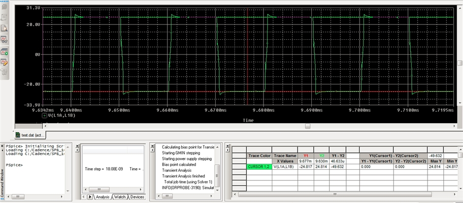
The voltage across the primary coil (L1a and L1b) will be a few voltages less than the specified input DC voltage, due to the voltage drop across the MOSFETs. Simulation results show the primary voltage as +/-24.8V (peak).

Figure 4: Voltage Across Primary Coils L1a and L1b

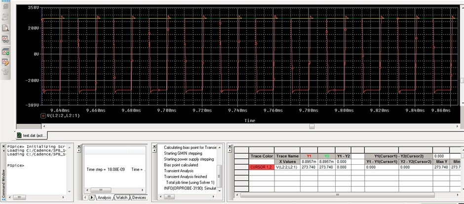
The secondary voltage will be around +/-273V (peak), since the turn ratio is considered as 11.
Simulation results show the secondary voltage as 273.74V (peak).

Figure 5: Voltage Across Secondary Coil

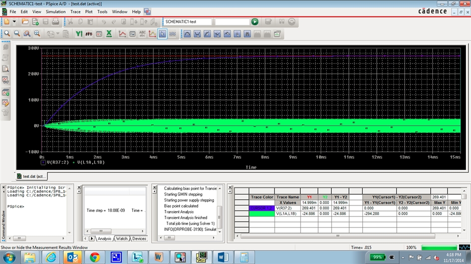
There would be a voltage drop across the rectifier diode. Simulation results show 269.4V DC at the output (R37).

Figure 6: Voltage Across Primary Coil (Green) and Load (Blue)

Refer to the complete app note* for a detailed procedure about each of the cycles described above and the necessary steps involved in the process.

* Note: The app note link can only be accessed by Cadence customers who have valid login credentials for Cadence Online Support (http://support.cadence.com).

Naveen Konchada

Power Integrity Solution Spans Multiple PCBs and Packages

$
0
0

When designing next-generation products, the common theme is "faster, smaller, cheaper".  When that is combined with longer battery life and lower power consumption requirements, the design challenges can be daunting.  And one thing you know for sure, the project schedule is not going to be extended to allow you to overcome all these challenges.

It certainly makes sense that every electronic product designer has a tool that enables analysis of the power delivery network.  While components can tolerate certain fluctuations in power and ground rails, there are limits to that tolerance.  Having planes that are so heavily perforated that they look like Swiss cheese and scraping away at fill areas to make room for signal routing are only going to exasperate the voltage fluctuations.  But when you're under the pressures of "faster, smaller, cheaper", these are the compromises that need to be evaluated.

DC power analysis, also known as IR drop analysis, is commonly the first tool electronic product designers will turn to when facing these challenges.  However, one common complaint has been that the analysis is done at a static temperature.   With the current returning through perforated planes and choke areas (neck down areas) in the plane, the current density and, therefore, temperature, are going to be higher than in other portions of the PCB where these conditions do not exist. So, analyzing IR drop at a static ambient temperature can lead to inaccurate IR drop predictions.  

Fortunately, there is a new trend, led by Cadence Sigrity PowerDC, where IR drop analysis is done concurrently with thermal analysis.  This allows the tool to predict the correct DC voltage drop based on the operating temperature of that region of the electronic product's PCB.  In addition to electrical-thermal co-simulation, Sigrity PowerDC is now capable of analyzing multi-board configurations.  So products that have memory cards attached can have the full system power delivery network analyzed.

If this sounds like something you would be interested in learning more about, please watch the 11-minute demonstration video below:

(Please visit the site to view this video)

We hope you found the demonstration informative. Sigrity PowerDC has been addressing complex power integrity problems for years, and continues to advance as a member of the Cadence Allegro Sigrity Integration (ASI) 16.6.1 product release.

Please do tell us about your experiences with PowerDC.

Team Allegro


Related stories:

Simultaneous Switching Noise Analysis - The Earlier the Better

Allegro Sigrity Makes its Debut at DesignCon 2013

Why Cadence Bought Sigrity - And How it May Change PCB Analysis

What's Good About Allegro PCB Editor Associative Dimensioning Updates? 16.6 Has Several New Enhancements!

$
0
0

With the 16.6 Allegro PCB Editor release, custom text can now be specified for any dimension value using the optional Text field located in the Options Panel. If the entered text is specified in the Text field, it will override any computed or specified entries in the Value field. You can also use the following format strings in the Text field:

  • %v when entered in the text field will be substituted by the computed dimension value
  • %u when entered in the text field will be substituted by units of IN or MM
  • To use a % character without special meaning in the text, use %%

If you enter the value 34.00 in the ‘Text’ field, it overrides the computed value of 4.43:


If you enter “length is %v %u, the resulting dimension value includes the prefix ‘length is’ before the computed value of 2.04. The suffix ‘IN’ is included as a result of adding %u to the text string:


Leader Lines: Leader line dimensions can now have optional text associated with them. If text is not desired, leave the text field blank. Entering text such as 'This is leader text' would result in:  
                <------- This is leader text

%n – add to text string if additional rows of text is desired

Example: 'This is line 1%nthis is line 2’
                <------- This is line 1
                          this is line 2

Balloon Dimensions: Instance parameter support is now available for balloon leaders. This allows different types of balloons (circles, squares …) to be used in the same design. 

Open an Allegro PCB Editor .brd file where you see some dimensioning and a balloon leader. Select Manufacture – Dimension Environment – RMB – Instance Parameters … (this step changes the circle balloon leader to square). Select the balloon circle. The ‘Instance Parameter’ form appears after the selection is made; click the ‘Balloons’ tab, then change ‘Type’ from ‘Circle’ to ‘Square’.

Balloon leader:

Override to square:


In the next few steps, we will override the dimension values with a combination of value and text strings. Add the word ‘TYP’ after the dimension 2.37. Select Manufacture – Dimension Environment – RMB – Change Text. Select the value ‘2.37’. Enter ‘%v TYP’ in the ‘Text’ field, then click ‘Enter’ or ‘Tab’:


Change the value 5.32 to 5.32 IN. Use the ‘Change Text’ command as you did in the above step. Select 5.32. Enter %v %u in the ‘Text’ field, then click ‘Enter’ or ‘Tab’. Add the prefix ‘my dimension’ when using the Linear Dimension command. Change the dimension command to Linear Dimension. Enter the text ‘my dimension %v’ in the ‘Text’ field.

Select the bottom edge of the board outline:  
                

Add a leader line with a 2 row text string. Manufacture – Dimension Environment – RMB – Leader Line. Enter a text string in the ‘Text Field’; ex – line 1 text%nline 2 text.

Make a LMB pick anywhere in the design to add the leader line:


As always, I look forward to your comments!

Jerry “GenPart” Grzenia

What's Good About Allegro PCB Editor Suppression of Unassigned Indirect Vias? 16.6 Has It!

$
0
0

The suppression of unassigned indirect vias is now supported in Allegro PCB Editor 16.6, which assigns the property ‘EMB_INDIRECT_VIA_SUPPRESS’ to the Component Definition, Component Instance, or Symbol Pin. If a component is placed on an ‘Indirect Attached’ embedded layer, this new property suppresses ALL via pads associated with the component if the PIN is not on a named net.  The indirect attach via pads will only be restored if:

  • The symbol pin changes to a named net
  • The symbol is moved to a layer which is not an indirect attach
  • The property is removed


Read on for more details …

Consider an Allegro PCB Editor .brd file with the following ‘Embedded Layer Setup’ form content, and review the strategy for this design:


Removing unassigned symbol vias is primarily done to free up space for routing.  Use Edit – Property and, as an example,  assign the property ‘emb_indirect_via_suppress’ to some BGAs. The property must be assigned to the ‘Component’ element in the database. Check your find filter:


Review the results noting the removal of several symbol vias on each component:


Delete the suppression property to ensure all symbol vias are restored. Move one of the components to an outer layer to ensure the original SMD pins are restored.

Please share your experiences using this new capability.

Jerry “GenPart” Grzenia

What's Good About the Allegro Design Entry HDL Front to Back Flow Cadence Training Course? Check Out this Video!

$
0
0

Hear what Bruce Imai—a Cadence Educational Services course developer—Cadence Application Engineers, and customers have to say about the valuable content available in our Allegro Design Entry HDL Front to Back Flow Cadence Training course. As Bruce emphasizes, “You’ll learn in a short amount of time techniques that might take you months to discover yourself.”

Here’s the video:
(Please visit the site to view this video)


The course is structured for both Design Engineers and PCB Layout Designers and has the following learning objectives:

  • Set up new projects
  • Create a flat, multi-sheet design
  • Check the design
  • Use part tables
  • Package a design
  • Create and customize a bill of materials
  • Build a hierarchical design
  • Use schematic properties to control part placement
  • Use the Constraint Manager to define high-speed routing requirements in Design Entry HDL
  • Transfer the design to the PCB Editor
  • Place parts manually
  • Auto-route with the PCB Router
  • Compare the schematic and layout
  • Synchronize design differences
  • Incorporate engineering changes
  • Link projects together in a team-design scenario
  • Reuse a hierarchical block and associated layout in another design

Learn more about this course and find additional information at our Cadence Training website.

I look forward to you sharing your experiences!

Jerry “GenPart” Grzenia

What's Good About Allegro PCB Editor Split Plane Association? 16.6 Has Several New Enhancements!

$
0
0

In the 16.6 Allegro PCB Editor release, net associations to split planes are now stored in the database. This reduces chance of error when re-generating split planes on positive or negative layers. The former use model required re-assignment of a net during the command, which was error prone and cumbersome.

When a split plane is regenerated, the net choice dialog for each shape is set to the default net that will be assigned to the shape. If you click ‘OK,’ it confirms the net assignment to the shape.  If you wish to select a different net, then select the ‘*’ in the drop-down and then select the correct shape.

If ‘Cancel’ is selected in the net selection dialog, a confirmer dialog with two choices will appear:

  • Click OK to allow the system to automatically assign nets to the remaining shapes based on database association
  • Click Cancel to set all remaining shapes to dummy nets


Read on for more details …   


Consider a PCB .brd file example with multiple signal layers. Enable the visibility of the GND_1 subclass including ‘Anti Etch’:


There are three split regions on this layer: GND, GND1, and 60V. We need to extend the existing split region to include J5-1. Select the ‘Delete’ command with the Find Filter adjusted to ‘Other Segment’. Delete the horizontal segment as shown below:


Invoke the Add – Line command, then adjust following the guidelines below:


Invoke Edit – Split Plane – Create to regenerate the split plane -
a.    Click to OK to simulate the pre-16.6 behavior mentioned. This could be quite tedious and error prone with large numbers of split regions.
b.    Click the ‘UNDO’ command to reset
c.    Now run the ‘Split Plane Create’ function once again
d.    This time, click the Cancel button, which invokes the dialog below:


e.    Click ‘OK’ to auto assign the net names

Please share your experiences using this capability.

Jerry “GenPart” Grzenia


What's Good or Not So Good About Cadence Documentation? Here’s Your Chance to Let Us Know!

$
0
0

Most of our customers use the product documentation, Help, and Cadence Online Support capabilities while using our products and flows. There is a team working on developing the next generation of Cadence documentation and the Help utility.

The Cadence Online Support - Cadence Support News area recently posted the following:
“Cadence is committed to providing high-quality documentation. To help us shape the future of Cadence documentation delivery we welcome you to complete our survey.


Here’s a direct link to the survey.


It would be great if you could take 10 minutes to complete the brief survey and help us review the areas where we can improve!

Jerry “GenPart” Grzenia

What's Good About Allegro PCB Editor Embedded Cavity DRCs? It's NEW in the 16.6 Release!

$
0
0

Max cavity size and max cavity component count were offered as reports in the 16.5 release and are now available as DRCs in the 16.6 release of Allegro PCB Editor. Fab houses supporting embedded component manufacturing offer design guidelines on cavity usage. 

Consider a PCB with the following characteristics. Layer SIGNAL_7 is displayed where you see two merged cavities on the left as the result of Cap placement combined with embedded parameter record #2 (min cavity gap for merging). There is one large cavity on the right associated with the BGA:

Select Setup – Constraints – Modes – Design Modes (Package) then enable the ‘Max cavity size’ and ‘Max cavity component’ count DRC mode:

Open the Design Options form:

  • Enter ‘3500’ for Max cavity size (units are sq mils)
  • Enter ‘4’ for max cavity comp count

Close form and note DRCs in the Allegro canvas:

Both DRC types are applicable to the column of Caps while the BGA cavity is greater than the specified 3500 sq mils. Move 1 cap from each column downward. We've resolved the max count issue, but still have an area issue:

Compress the placement using the new Component Alignment features. (Equal or DFA spacing):

No action is required on resolving the BGA DRC.  This might require an edit to the symbol definition to meet the rule. Manually draw a ‘super cavity’ around all 10 Caps. This is done using:

  • Shape – Manual/Void Cavity
  • Select Polygon
  • Select any part of the yellow cavity shape
  • Draw Polygon

New DRCs should be generated:

Delete the manually drawn cavity:

  • Select Shape – Manual/Void Cavity
  • Select ‘Delete’ from the pull-right menu
  • Make a pick on the void outline of the cavity to delete it

I welcome your feedback!

Jerry “GenPart” Grzenia

What's Good About Allegro PCB Editor Disable of Open Space Routing? 16.6 Has It!

$
0
0

By default, the 16.6 Allegro PCB Editor‘Add Connect’ command generates routes when a pick is made on database elements like pins or vias, but also when a pick is made in open or black space. Designers who push the mouse fast and hard frequently make false picks and are forced to opt out of the command then refine the pick to a logical element like a pin or rat line. Some designers may embrace the open space pick concept when interconnect strategies call for partial routing of buses or interfaces. Since there is no clear preference on default behavior, a solution driven by a user preference variable is offered. When enabled, the Add Connect command would reject any picks made that are not associated with database elements like rat lines, pins, vias, segments or shapes. The variable setting does not affect ‘multi-line’ route which is designed to work by making a pick in open space.


Variable: User Preference Editor – Route – Connect – ‘acon_disable_nullnet_route’


Read on for more details …


Invoke the ‘User Preference Editor’ (Setup – User Preferences). Open the Route – Connect folder then enable the variable ‘acon_disable_nullnet_route’. Setting this variable does not require the Allegro tool to be restarted. Invoke the ‘Add Connect’ command then try to make a pick in open space. Note the command window messaging informing you ‘no element was found’:


Please share your experiences using this new capability.

Jerry “GenPart” Grzenia

What's Good About Allegro PCB Editor DRC by Window? It’s in the 16.6 Release!

$
0
0

The 16.6 Allegro PCB Editor‘DRC by Window’ command is an alternative to running DRC update at the full design level. As the name suggests, the command is limited to checking the elements within the extents of a user-defined selection window. On large, highly constrained designs where database performance is problematic, one can simply disable ‘On-line’ DRC mode if favor of this ‘On-demand’ method.

The ‘DRC by Window’ command is located in Tools – Window DRC or available from the Toolbar  


Read on for more details…


Disable the Online-DRC system. There are a couple of methods to consider:

  • Setup – Enable Online DRC
  • Display – Status
  • Setup – Constraints – Modes


               Setup menu                                             Status menu                                                            Constraint modes

The DRC mode status can be obtained by hovering over the banner field in the lower right corner:


Move a few components; slide a few routes with the intent of creating DRCs.
Select the Icon to run the ‘DRC by Window’ command then window around elements as appropriate to update the DRC status for that area:


Noteson ‘DRC by Window’:

  • Use in conjunction with the Find Filter elements
  • Heads-Up Display is still active even though Online DRC is disabled
  • If ‘Net’ is selected in the Find Filter, DRCs may be produced outside the window’s extents as the DRC will walk the elements associated with the net


I look forward to your input!

Jerry “GenPart” Grzenia

What's Good About Allegro PCB Editor NC Route? 16.6 has Several New Enhancements!

$
0
0

There are a few NC Route enhancements in the 16.6 Allegro PCB Editor release.

Read on for more details …

Separate plated vs. non-plated files

An option has been added to the NC Route user interface to specify that separate output files are desired for plated versus non-plated routing. When this option is enabled, non-plated routing for both the board and slot holes will continue to be output to a ‘<name>.rou’ file, while plated routing for both the board and slot holes will now be output to a new ‘<name>_plated.rou’ file.

When disabled, all NC Routes will continue to be output to the single ‘<name>.rou’ file:


Auto-generate tool codes and sizes

The current NC Route functionality requires that the user supply an ‘ncroutebits.txt’ file that specifies the EXCELLON format tool codes and sizes that will be needed for the routing of board paths and/or slot holes of a design. This requires that the user has detailed knowledge of the routing requirements of the design, and also that the tool sizes need to be specified in the EXCELLON format output units as opposed to the more familiar units of the design in question.

In 16.6, if an ‘ncroutebits.txt’ file is NOT found, the tool code and size information will be automatically determined and used. The information will also be output to an ‘ncroutebits_auto.txt’ file for reference, similar to the ‘nc_tools_auto.txt’ file generated by NC Drill in the same situation. The ‘ncroutebits_auto.txt’ file itself will never be read as currently named by NC Route. It could be renamed though to ‘ncroutebits.txt’ for any subsequent executions of NC Route to bypass the auto-generation.

Open an Allegro PCB Editor .brd file. Run the ‘NC Route’ application from Manufacture – NC – NC Route. Enable the new option ‘Separate files for plated/non-plated routing’:


Click on the ‘Route’ button. Use ‘File – File Viewer’ to access the files:


Open the ‘ncroutebit_auto.txt’ file noting the tooling codes:


I look forward to your feedback.

Jerry “GenPart” Grzenia

What's Good About Allegro PCB Editor Line Width Retention? 16.6 Has It!

$
0
0

Currently, user line width overrides are permitted during the Add Connect command, but are reset back to constraint driven when the command is completed. New behavior in the Allegro PCB Editor 16.6 release maintains the user setting until it is manually reset. The line width override now appears in blue, similar to the model established in the Constraint Manager Worksheets or shape parameter form to represent an override state. The user can easily reset to constraint mode by selecting constraint from the drop-down menu.

Open an Allegro PCB Editor .brd file and invoke the ‘Add Connect’ command then open the Options Panel. Enter a value in the ‘Line Width’ field; 12 for example. Note the color change to blue, a format that is recognized by Allegro users as an override state:


Route any connection in the workspace then perform a RMB – Done.

Re-invoke ‘Add Connect’, noting the 12mil value has been retained. Prior to 16.6, the value would be aligned with the constraint driving line width for the net about to be routed.

User comments in the past suggest the constant resetting of line widths to be frustrating, but something they just live with. This is mainly heard from designers responsible for analog routing where sometimes, the design rule is ‘route as wide as possible’.

Choose a ‘Line width’, then select ‘Constraint’ to resume Constraint Driven routing.

Please share your experiences using this capability.

Jerry “GenPart” Grzenia

What's Good About Allegro PCB Editor Replace Padstack? 16.6 Has Several New Enhancements!

$
0
0

The Allegro PCB Editor 16.6 ‘Replace Padstack’ command is now available as a context menu item when the selection set consists of mixed padstack instances.  Prior to 16.6, the selection set would have to be limited to common padstacks. This is available in General Edit Application mode.

Read on for more details …

The Options Panel now supports the ‘Ignore FIXED property’. The ‘Pin Number’ field has been enhanced to support a range of values:


I look forward to your feedback.


Jerry “GenPart” Grzenia


What's Good About Allegro PCB Editor Pastemask DRC? 16.6 Has Several New Enhancements!

$
0
0

The Allegro PCB Editor 16.6 Pastemask to Pastemask DRC now checks the ‘Package Geometry - Pastemask_Top’ shapes within the same symbol.

Read on for more details …


In Allegro PCB Editor, open a library symbol (e.g. pastemaskdrc.dra). Enable Pastemask DRC mode.

Setup – Constraints – Design Modes (Soldermask):


Open the Design Options (Soldermask) form and enter a value of 10 for Pastemask to Pastemask spacing:


Enhanced DRC now detects shape-to-shape spacing within same symbol:


I look forward to your feedback.


Jerry “GenPart” Grzenia

What's Good About Allegro PCB Editor Symbol Editor? 16.6 Has a Couple of New Enhancements!

$
0
0
The Allegro PCB Editor release has a few new capabilities related to symbol pins. The Symbol Editor has been enhanced with a new utility designed to automatically renumber pins based on positional qualifiers. The path to the utility is ‘Layout –...(read more)

What's Good About Cadence PCB Design and SI/PI Analysis Products? The 16.6 release has QIRs!

$
0
0

I’m taking a brief detour from the usual product technical details this week to mention (and in most cases – remind people) that the Cadence PCB Design and SI/PI Analysis Products provide Quarterly Incremental Releases – or QIRs. You can find brief descriptions of what’s contained in each QIR here. Near the bottom of each main product section (Allegro, Sigrity, OrCad) there is a “What’s New” link. Selecting this will provide you more details about specific QIRs. Here’s the "What's New" link for Allegro PCB Editor.

While the word “incremental” denotes a small change, some of these QIR releases contain significant product technology advancements that are typically found in our major releases. We’ve provided QIRs for a few years now so that you can benefit from these new product features and enhancements on a more frequent basis instead of waiting for months or years before being able to use the capabilities.

I will be blogging about the details of the 16.6 QIRs over the coming weeks and months. I’ll start with the most recent QIR (QIR #9 or better known as 16.6–2015 Release) and work backwards to earlier QIR releases (QIR #8, QIR #7, … QIR #1). While this may seem odd, my goal is to relate the most current and impactful product capabilities first from the latest QIR so you can utilize these in your design environment. Some blog posts will contain just a brief list of product and flow features available in the QIR (with references to details on Cadence Online Support) and others will provide in-depth descriptions of functionality.

My goal is to provide you the most relevant product details so that you can achieve maximum efficiency and productivity.

Here are just a few topics I’ll be writing blog posts –

Allegro PCB Editor

  • Allegro PCB Designer Manufacturing Option (DFM Checker, Documentation Editor, Panel Editor)
  • Allegro Relational Rules Checker (running RAVEL rules)
  • Differential Pair Return Path Vias
  • Fiber Weave Effect - Zig-Zag Routing
  • Auto-Interactive Adjust Spacing
  • Auto-Interactive Swap Pins (Design Planning Product Option)
  • Productivity Enhancements (new shape editing mode, persistent snap and selection, island permanent highlight, and much more)


Allegro Design Authoring

  • Variant Editor enhancements (hierarchical variants, schematic editor dynamic viewing, capturing variants on the schematic)
  • Online Component Browser support for non-ADW projects
  • Tag-based ECSet Mapping


Allegro Design Workbench

  • Using Component Browser with Project Manager projects
  • ADW Server Error Logging and Notification
  • Enhancements in Library Import
  • Condensed Library Flow


Allegro FPGA System Planner

  • Managing Design Block Symbol
  • Generating an ASA Design
  • Enhanced Multi-Device Connections (Daisy Chain Connectivity)
  • Termination Reference Designator Support (OrCAD)


OrCAD Capture / PSpice

  • Enhancement in Learning PSpice
  • Enhancement in the Capture Start Page
  • New Simulation Macro Models for the Capture-PSpice Flow
  • VBIC Support added in PSpice
  • ADMS XML filters for Verilog-A to PSpice DMI Models Translation


SiP

  • Co-Design Die Editing in Symbol Edit Application Mode
  • Defining Variants
  • Replacing Via with Via Structure
  • Exporting Netlists
  • Degassing Enhancement of Void Clearance for Adjacent Layer Shapes


Jerry “GenPart” Grzenia

What's Good About the DEHDL Variant Editor? The Secret's in the 16.6 Release!

$
0
0

The 16.6–2015 (also known as 16.6 QIR#9) Design Entry HDL (DEHDL) release contains upgraded capabilities for the Variant Editor – namely:

  • Dynamic viewing of variants in the schematic editor
  • Capturing variants on schematics
  • Replacing a part with any other part using the Component Browser
  • Support for hierarchical variants


Here are a couple videos detailing these new capabilities.

Read on for more details…


Dynamic viewing of variants in the schematic editor

A new toolbar and menus have been added for viewing variants. All available variants for the design are listed and the selection of a variant leads to the annotation of variant-specific information (properties) on the schematic sheets (e.g. Do Not Install, Option to Cross Out). It’s easy to switch between any of the variants as well as base views:


True hierarchical schematic support is now available with occurrence-specific data and Cross Referencer data present in plots/PDF Publishing of any of the variants with complete data. User-defined properties/custom text can be assigned variant-specific data in the Variant Editor (placeholders on schematics are updated with variant-specific data).

The Attribute form displays the variant name in the source column for variant-specific properties:


There is an option on DNI Components -
Cross Out
DNI Property
All Properties Visibility

There is also color customization -
Variant Specific Component    
Variant Specific Properties
DNI Component    
DNI Cross


When you perform a Save in the Variant Editor, it generates files specific to each variant containing variant-specific information. These files are used for dynamic display of data in DEHDL schematics.

The variant details can be defined at the time of creating a new variant or editing existing variant details -
Variant Name
Variant Property Name-Value to be annotated on schematics
DNI property value
Variant-specific Custom Text values

Special characters [/, ., =, <, >, /, +, (, )] are now supported in the variant name and property values:


Capturing variants on schematics

Features available in the schematic Base View:
Create Variant
Edit Variant
Remove Variant
Launch Variant Editor
View Schematic Variant
Mark for Variant


Features available in Schematic Variant View:
Launch Variant Editor
View Schematic Variant
Mark for Variant
Remove from Variant
Mark as Do Not Install
Make Preferred
Modify Component
Add Alternate
Modify Properties


When you create a new variant, the new variant dialog box appears and is pre-seeded with entries from the project and/or site .cpm file -
Variant Property Name
Variant Property Value
DNI Value
Custom Variables
Specify Variant Name


Modify any of the pre-seeded data, click OK, and the new variant is created and can be viewed in the Variant Editor. The DEHDL menus get updated to allow working on the new variant. You can edit and remove a variant as well. Launching the Variant Editor displays all the variant details:


You can mark part instances for variant(s) by selecting one of more packaged instances on the schematic and mark them for variant(s). A context menu also available on instance(s). When block instance(s) are selected, the command operates on packaged instances of the block instances which are not packaged are ignored for all variant operations:


When you’re in the schematic base view, a sub-menu shows all the available variants for selection. You have the option to select multiple variants and mark them. When you’re in the schematic variant view, only the current variant is shown in the sub-menu. Selected instance(s) are added to a variant and can be seen in the Variant Editor. When an instance(s) is part of a function or group, then a message is reported and that instance is ignored.

The Remove from Variant is available in the schematic variant view. You can select one of more instances on schematic which are part of the variant and remove them. A context menu is also available on instance(s). When block instance(s) are selected, the command operates on packaged instances of the block. When instance(s) is not part of the variant, then a message is reported and that instance is ignored. When instance(s) is part of a function or group, then a message is reported and that instance is ignored.

The Mark as Do Not Install is available in the schematic variant view. You can select one of more instances on schematic and mark them as DNI. A context menu is also available on instance(s). When block instance(s) are selected, the command operates on packaged instances of the block. When instance(s) are not part of variant, they are added to the variant and marked DNI. When instance(s) is part of a function or group, then the message is reported and that instance is ignored.

The Make Preferred is available in the schematic variant view. You can select one or more instances on schematic and mark them as Preferred. A context menu is also available on instance(s). This does not work on block instance(s). When instance(s) are not part of a variant, they are added to the variant. When an instance(s) has been modified (part of a function or group or has a changed value or modified), then a message is reported and that instance is ignored.

The Modify Component is available in the schematic variant view. You can select one or more instances on schematic and modify them. A context menu is also available on instance(s). It works on the same logical components, but does not work on block instance(s). When instance(s) are not part of a variant, they are added to the variant and modified. Part Table rows corresponding to the part are displayed for a new selection. The footprint of a newly selected component should be compatible with the original footprint. When an instance(s) is part of a function or group or has a DNI status, then a message is reported and that instance is ignored.

The Add Alternate is available in the schematic variant view. You can select one instance on the schematic and add an alternate for it. A context menu is also available on the instance. It does not work on block instance(s). When an instance is not part of a variant, it is added to the variant and an alternate is added. Part Table rows corresponding to the part are displayed for an alternate selection. When an instance is part of a function or group or has DNI status, then a message is reported and that instance is ignored.

The Modify Properties is available in the schematic variant view. You can select one instance on the schematic and Modify Properties for it. A context menu is also available on the instance. It does not work on block instance(s). Properties are added/modified specific to a variant for a selected instance. Property names to be displayed can be configured using a .cpm file directive. When an instance is part of a function or group or has DNI status, then a message is reported and that instance is ignored.

Replacing a part with any other part using the Component Browser

You have the ability to replace a part by selecting any part using the Component Browser:


Verification ID is performed to check that the selected replacement part has the same footprint (JEDEC_TYPE property) and a compatible footprint file (\cdssetup\cjedectype.txt):


There is an option to run custom code for further verification of the replacement part:
Script File path can be specified using a project .cpm file directive
Script File takes footprint names (Original and New) as Input
Script File generates a log file which can be viewed
Script File returns code, which is displayed

You still have an option to continue replacing with the part not having a compatible footprint. The variant BOM reports display information about the replaced part. You can specify Replacement Component by just specifying a KEY property value for a new part. The property name can be configured using a .cpm file directive. You also have an option to specify a replacement component with no part table entry (this is useful for programmable devices).

Support for hierarchical variants

The variant definition from lower level hierarchical blocks is available for use at the top level. A one time import of variant data is required. The Variant Editor view changes to show the instances part of the lower level variant as separate groups / functions. There is the ability to include a variant coming from a lower level block in the top-level variant and the ability to mark the complete block instance as DNI. There is an option to generate hierarchical BOM reports (with a single entry for each block instance, and components coming from a block instance excluded from the main BOM).

You have the ability to apply variants on block Instances. Variants defined inside a block are available for application on the block instance. Block variants can be specified on instances of Reuse Blocks only. Block Names are defined in the USE_SUBDESIGN or FORCE_SUBDESIGN directives. An additional property can be identified which needs to be present on the block instance for enabling the hierarchical variant application (the property name can be configured using a .cpm file directive):


The hierarchical variant BOM report generated for a design displays a single entry for a block instance, the block name, the SUBDESIGN_SUFFIX property value for identifying the block instance, the applied variant name, and any variant-specific properties. The applied variant data is visible on the schematic canvas and in the Variant Editor. When a block instance is marked DNI, it is removed from the hierarchical variant BOM report.

Each block has its own BOM report which can be referenced from the root design BOM Report. There is an option to generate a hierarchical BOM report available as a check box in the BOM UI. The report contains a single entry for each block instance. Only reuse blocks are listed as hierarchical block instances. Block names are defined in the USE_SUBDESIGN or FORCE_SUBDESIGN directives. Components coming from a block instance are excluded from the BOM report. An additional property can be specified for identifying hierarchical block instances. Properties on a block instance can be part of the BOM report:


Please share your experience using these new features.

Jerry “GenPart” Grzenia

What's Good About Allegro PCB Designer Manufacturing Option? It's NEW in the 16.6 Release!

$
0
0

Wow! There is an extremely powerful option available for PCB designers in the 16.6 - 2015 Allegro PCB Editor release—the Allegro PCB Designer Manufacturing Option. This option is integrated into the Allegro PCB Editor.

As you’ll read in our “What’s New” section, “The Allegro PCB Designer Manufacturing Option is a comprehensive, powerful, easy-to-use suite of tools that makes it efficient for PCB designers to streamline the development of release-to-manufacturing packages for their products. It includes three modules: Design for Manufacturing (DFM) Checker, Documentation Editor, and Panel Editor.”

DFM Checker

Allegro PCB Designer Manufacturing Option’s DFM Checker module is a suite of manufacturing analysis tools that helps engineers and designers ensure no fabrication-related issues are present before sending the design off for fabrication, thereby helping to avoiding fabrication-related delays, additional costs, and re-work. You will catch violations before releasing to manufacturing.

  • You can consider the various analysis capabilities as a “second set of eyes” for fabrication checks. It includes IPC-2581 standard checking, multiple rules check options, and rules by group (streams).
  • You can import physical and region constraint values and manufacturers rule sets templates and setup default physical check values.
  • The checks can be run in the background—Allegro PCB Editor and Documentation Editor can be used while checks are running!
  • In the results review form, any resulting violations are listed by check category and you can crossprobe the violations between the violations list and Allegro PCB Editor:

 Allegro PCB Designer Manufacturing Option’s DFM Checker module

Documentation Editor

 Documentation Editor

Allegro PCB Designer Manufacturing Option’s Documentation Editor module is a PCB documentation-authoring tool that intelligently automates your documentation creation process to produce complex PCB documentation in a fraction of the time versus traditional methods. Documentation Editor enables you to quickly create the manufacturing drawings that drive PCB fabrication and assembly. It provides customizable templates and scripting capabilities.
 Drill Chart


  • Document types generated include Fabrication, Assembly, and Custom document.
  • There is a page setup where you specify standard document sizes as well as a document template that adapts to page sizes.
  • The template library includes Legends, Notes, and Details.
  • The data import contains Drill Legend, Stack-up, and Assembly BOM.
  • Dimensioning capabilities for Linear, Datum, Tolerance, Dual Inch/mm values.
  • Drawing details provide Detail magnification tools and Detail templates
  • Some of the export options are BOM export (.csv list, and .txt file), Placement Coordinate List, PDF Document, and DXF Export.


 Detail magnification tool       Detail template


Panel Editor

Allegro PCB Designer Manufacturing Option’s Panel Editor module intelligently automates the complex process of panel definition and documentation, simplifying the design process. This solution enables designers to quickly create electronic manufacturing documents that clearly articulate the panel specification and instructions for successful fabrication, assembly, and inspection of their designs.

  • Assembly Panel Creation generates the assembly panel size and calculates the layup.
  • Panel tooling definition quickly defines milling definition panel pinning holes and panel detail
  • Panel documentation includes the drawing details, notes and a drill/assembly legend.
  • You can export a .pdf document and a .dxf file.

 Panel Editor

I look forward to your feedback!

Jerry “GenPart” Grzenia

Viewing all 663 articles
Browse latest View live


<script src="https://jsc.adskeeper.com/r/s/rssing.com.1596347.js" async> </script>