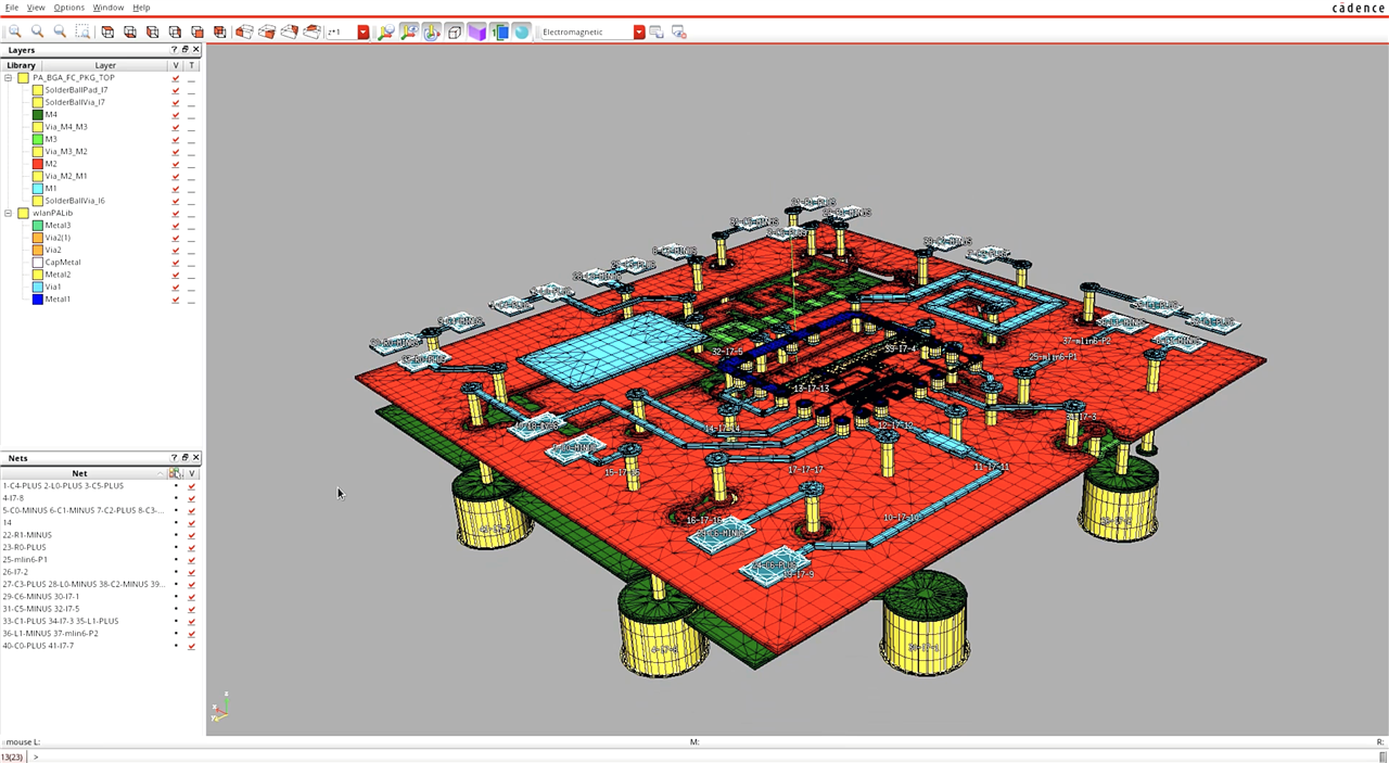
By John Park, Product Management Group Director for Advanced IC Packaging, Cadence
Traditionally, the integration process involving chips, packages, and PCBs relied heavily on manual methods. Experts in different areas—such as IC, PCB, and packaging— used specialized tools for their particular segment, leading to a compartmentalized approach to design. Engineers soon realized that this method of working in silos would not achieve the best possible outcomes for the next generation of analog/RF circuit designs with multiple dies.
Introduction of Co-Design Needs for Multi-Die Packages
Until recently, the field lacked a streamlined and automated method for concurrently designing across domains. Co-design is now possible through modern software that combines IC design, various heterogeneous dies, packaging solutions, and PCB design environments. Platforms must facilitate a unified and automated workflow across IC, package, and PCB design stages, streamlining the process, speeding up design cycles, and reducing the likelihood of errors.

Shorten design cycle and expedite time to market with Virtuoso heterogeneous integration
Why Is Co-Design for Multi-Die Packages Important?
Designers need a systematic and automated system for co-design and co-analysis for a multitude of reasons:
1. To reduce the margin for human error
2. To analyze the entire system and interactions between the ICs, dies, their package, and their PCB
3. To conserve the time and effort it takes to create systems that perform better and are more cost-effective
Designing for Multiple Die Packages
The process of combining multiple dies within a single package presents distinct challenges different from that of a single unified die. Each component may be developed at the same technological node but utilizes a different manufacturing process. With the move towards more diverse and separated design architectures, components need to be co-designed as part of a whole system. This includes meticulous modeling, floor planning, verification, and debugging efforts to ensure functionality.
This is where the importance of packaging comes in: it is essential to confirm that Chiplet A correctly interfaces with Chiplet B through their shared packaging, marking a significant pivot towards system-level design practices. In creating the optimal package configuration, careful consideration must be taken for key elements like GPUs, CPUs, and I/O interfaces. An advanced package must be able to house various dies, each possibly utilizing distinct process technologies and serving different functions.
Optimal performance, cost reduction, and accelerated time to market hinge on effective cross-domain co-design and co-analysis. The Cadence Virtuoso Studio delivers these crucial capabilities by seamlessly integrating IC design into Allegro X Advanced Package Designer and Sigrity signal and power integrity technology. This advanced technology establishes a streamlined and automated design flow, resulting in a more efficient overall design journey. Cadence’s upcoming talk at the IMAPS Device Packaging Conference will aim to discuss many of these issues, solutions, and more.
Cadence’s Upcoming Talk at IMAPS Conference: Co-Design of Analog and RF Multi-Die Packages
As the industry shifts towards heterogeneous design assembly, there will be many notable transformations within analog and RF multi-die packaging. Among these transformations, designers will be impacted by the future shape of co-design, and as packages will contain multiple dies, designers will be tasked with analyzing and characterizing these packages for the behavior and performance of analog/RF circuits.
This talk will explore the evolving trends and challenges within analog/RF multi-die packaging and propose potential strategies for effectively co-designing and co-analyzing interactions among ICs and chiplets, advanced packaging, and PCBs.
About the IMAPS Device Packaging Conference
The Device Packaging Conference serves as a platform for knowledge exchange, offering a variety of technical sessions, social events, and networking opportunities with top experts in the field. This event will draw a variety of participants from both industry and academia, fostering educational interactions among diverse functional groups and various levels of experience.
Beneficiaries of this conference encompass a range of professionals including scientists, process engineers, product engineers, manufacturing engineers, professors, students, business managers, as well as sales and marketing professionals. The conference will feature three tracks with 12 technical sessions and over 100 speakers. The tracks include:
1. Heterogeneous 2D & 3D Integration Track
2. Fan-Out, Wafer/Panel Level, and Flip Chip Packaging Track
3. Next-Gen Applications Track
Sign Up for the IMAPS Packaging Conference
In its 20th year, the Device Packaging Conference (DPC 2024) is scheduled to take place at the WeKoPa Resort and Conference Center from March 18th to 21st, 2024. This global gathering is orchestrated by the International Microelectronics Assembly and Packaging Society (IMAPS). Register now to join industry leaders at this important conference.
Leading electronics providers rely on Cadence products to optimize power, space, and energy needs for a wide variety of market applications. To learn more about our innovative solutions, talk to our team of experts.