Several new features have been added to the 16.6-2015 SiP release.
Read on for more details …
Co-Design Die Editing in Symbol Edit Application Mode
The Symbol Edit Application Mode has been expanded to operate on co-design dies as well. A co-design die is one that was created by the loading of a die abstract. Using the Symbol Edit Application mode, you can refresh a co-design die symbol and also view and edit die bumps and I/O drivers: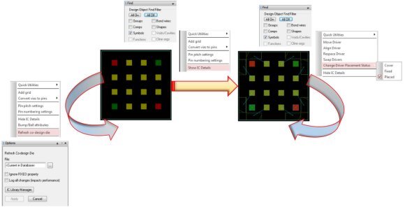
Using the new options, you can easily balance the ideal bump pattern with respect to both the drivers and top level metal in the IC and the pin escape pattern on the package substrate, or bond wire pattern for a bonded die; for example, you can optimize the bump pattern with respect to both the drivers and the package pins or optimize net assignments.
Use the Refresh co-design die option to refresh a die in the database from the disk file or to make a library change.
After displaying the I/O drivers of a co-design die using Show IC Details, you can perform the following operations on the selected drivers:
- Move
- Align
- Respace
- Swap
- Change Driver Placement Status
Defining Variants
You can now define subsets of components and cross-section layers in a master design so that each subset is a single variant of that package design (Manufacture - Define Variants). For example, you might define two variations of a memory stacked design, where each variant has memory chips from a different set of vendors. Using the variants feature, you can create a master design that contains the dies for the different variants, and then define a variant for each set of dies which will be assembled together in a final, packaged substrate.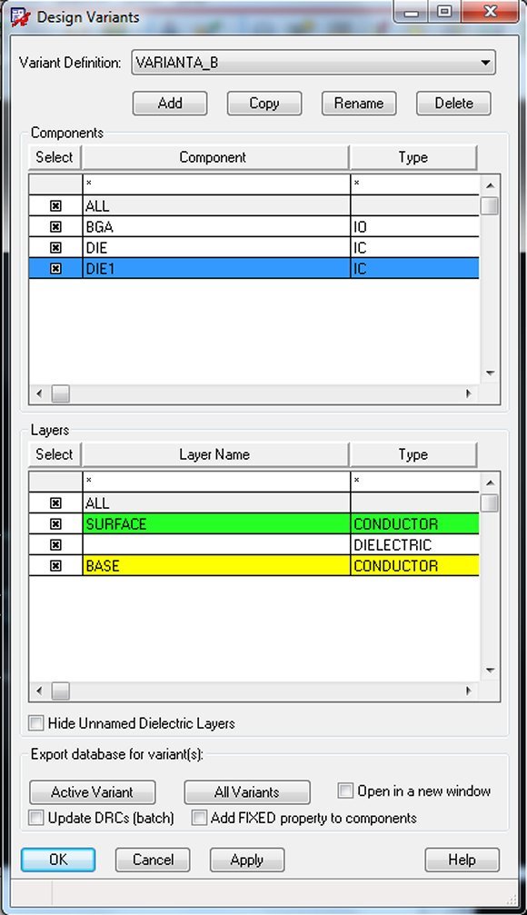
This feature saves design time by allowing you to design once, and then analyze and manufacture many times; you manage all physical connections in a master design and then generate variant designs that are ready for SI and PI analyses, 3D DRCs, and documentation generation.
By using the variants feature, you ensure that when the package substrate is updated, all the variants are updated; decreasing the chances of synchronization and manufacturing or assembly errors. For example, when pushing and shoving a bond finger in the master drawing, all bond wires connecting from any of the variants' dies are updated at the same time. Similarly, if a new finger is added such as a blank bonding target in some variants, the finger label of all variants are updated and geometries exposed through soldermask openings are kept in sync. The overall impact is a greatly reduced probability of errors during manufacturing or assembly of any of the final packaged components.
Replacing Via with Via Structure
You can now create as detailed a via pattern as necessary in an efficient, quicker way while performing interactive routing. Use the new replace via with via structure command to replace selected or all vias that use a specific padstack definition with instances of an existing via structure definition. For example, use a large via, which reserves the space needed for a more complex via structure pattern, during initial routing. When routing is complete, replace the placeholder via with the via structure to create the final, detailed routing.
You can also use this command to replace instances of a via structure with a via in order to restore the design to its original state with the original vias.
Changing Symbol Owner
You can now interactively add static shapes as children of a symbol instance. For example, you can add texts, fiducial vias, alignment lines, or reference outlines or shapes. Any operation, such as move or delete, performed on the parent symbol instance will also occur on the children.
Note: If you refresh a symbol from library, any instance items will be be deleted. If you want the instance items to be preserved, disassociate the instance items first and then reattach them after refresh.
Use the change sym owner command either to add database objects as children of a specified symbol instance or to remove current children from their owning parent symbol instance.
Exporting Netlists
You can use the netlist spreadsheet command to export a spreadsheet style netlist to be used for documentation purposes. The spreadsheet is organized as a set of columns for each component: any BGA components, followed by die components, and, finally, discrete components. The cells are colored according to the color of the nets in the design. The spreadsheet contains columns for Net name, RefDes, Pin Number, and Pin Name.
Degassing Enhancement of Void Clearance for Adjacent Layer Shapes
You can now specify the behavior of degassing void creation depending on overlap with adjacent layer shapes using the new Adj. layer void clearance option. Earlier, shapes on adjacent layers were ignored by degassing. Now, in addition to the default behavior that ignores adjacent layers, you can also specify the following behavior by selecting the appropriate option:
- Inside Shape: Degassing voids will only be created if the void is entirely inside an adjacent layer plane shape.
- No Void Overlap: Degassing voids will not be created if there is an overlap with a void in another shape.
Please share your experiences using these new capabilities.
Jerry “GenPart” Grzenia